
Minister Sridhar Babu Launches India’s First Chemical Mechanical Polishing Technology Centre at T-Works
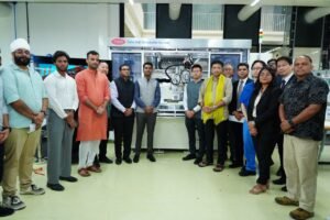
THE JOURNALIST POST | HYDERABAD | July 11
Telangana marked a major milestone in India’s semiconductor journey with the inauguration of the country’s first Chemical Mechanical Polishing (CMP) Pad Technologies Hub at T-Works in Hyderabad. The state-of-the-art facility was formally inaugurated on Saturday by Telangana Minister for Information Technology and Industries Duddilla Sridhar Babu.
The hub has been established through a collaboration between T-Works and Toho Koki Seisakusho Co. Ltd. of Japan, marking the first time that CMP pad technology has been introduced in India.Addressing the gathering, Minister Sridhar Babu said the Telangana Government is implementing a well-defined strategy to transform the state into one of India’s leading semiconductor manufacturing destinations. He described the CMP Pad Technologies Hub as a significant addition to the state’s rapidly growing semiconductor ecosystem.Chemical Mechanical Polishing (CMP) pads are critical consumables used in semiconductor manufacturing to achieve ultra-flat wafer surfaces during chip fabrication. Until now, India depended entirely on imports for this technology. With the launch of the new hub, Hyderabad has become the country’s first centre for CMP pad technology, reducing dependence on foreign expertise and strengthening India’s semiconductor capabilities.
The Minister said the facility will serve as a centre for advanced training, technical research, innovation, and product development. Students, researchers, startups, MSMEs, and industries will receive hands-on training and technical support through the hub. Collaborative research programmes will also be undertaken with premier educational institutions, research organisations, and industry partners.He expressed confidence that India would be able to manufacture CMP pads domestically within the next 18 to 24 months, significantly boosting the country’s semiconductor supply chain.
Highlighting Telangana’s global partnerships, the Minister said the state is working closely with Japan and other technology-leading nations to bring advanced semiconductor technologies to India. He added that the government is preparing a comprehensive roadmap to build a complete semiconductor ecosystem in Telangana, spanning research, innovation, manufacturing, and advanced chip production.The inauguration ceremony was attended by Takuya Nishimura, Swastik Kulkarni, Daisuke Tanji, Shigemaro Yasui, Anudeep Durishetty, Joginder Tanikella, senior government officials, industry representatives, researchers, and technology experts.